Channels
Special Offers & Promotions
Cameca Launches Eikos-Uv
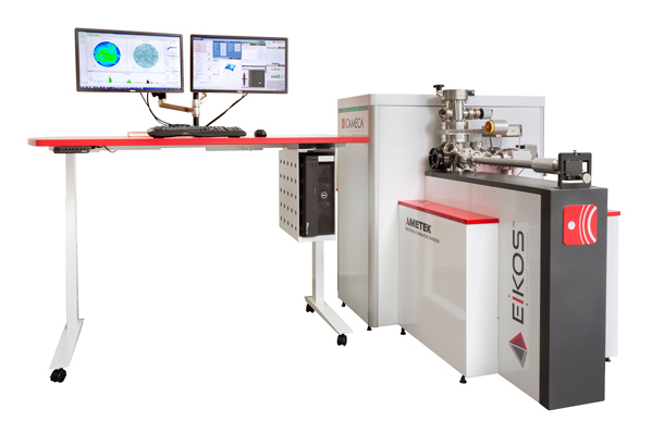
AMETEK CAMECA, a world leader in scientific instrumentation and metrology solutions, is pleased to announce the release of EIKOS-UV, a new atom probe microscope.
EIKOS-UV is a workhorse Atom Probe Microscope with increased ease of use and a low cost of ownership. Utilizing standard microscopy sample preparation methods, it delivers nanoscale structural information, enabling new a understanding of materials for research and faster development of products for industrial applications.
“CAMECA is very proud to introduce EIKOS-UV,” said Dr. Jesse Olson, CAMECA Business Unit Manager. “We believe that with both the voltage pulsed mode and UV-laser pulsed mode, the EIKOS-UV will bring Atom Probe Tomography within the reach of many new microscopists, researchers and engineers, allowing them to image their materials at the atomic level.”
Olson continued, “CAMECA builds on over 30 years of success in Atom Probe Tomography instrumentation and applications development to deliver the new EIKOS-UV platform, which we designed to maximize utility for the development of commercial alloys and essential research at the university level. The design, layout and footprint of the EIKOS-UV provide flexibility for site requirements, while high reliability and ease of use are made possible thanks to two major instrumental innovations: an integrated pre-aligned electrode that eliminates the need for in-situ alignment, and a new 355nm laser pulse system.”
EIKOS-UV addresses a wide variety of applications including metals, semiconductors, functional materials, minerals, nuclear structural materials, thin films and coatings. Its standard specimen preparation methods and mature data analysis routines make it a cost-effective workhorse instrument for nanoscale materials research and industrial materials development, and a valuable addition to CAMECA’s Atom Probe Tomography product line.
EIKOS-UV is available in two configurations. The first is the base EIKOS system, which incorporates a reflectron spectrometer design to provide excellent mass resolving power and signal to noise with a voltage pulsing system to ensure very high data quality on a wide variety of metallurgical applications. The second is the fully configured EIKOS-UV system, which adds an integrated, automated laser pulsing module with computer controlled focused spot design to provide access to a larger application range and even higher signal to noise. The base EIKOS system is field upgradable to the EIKOS-UV.
Atom Probe Tomography (APT or 3D APT) is the only materials analysis technique offering extensive capability for both 3D spatial imaging and chemical composition measurements at the atomic scale. Since its development in the 1960s, the technique has contributed to major advances in materials science. Exclusively developed and manufactured by CAMECA, Atom Probe Microscopes are used by prestigious research and development laboratories around the world.
The CAMECA Atom Probe Tomography product line now comprises two families: the LEAP 5000 (Local Electrode Atom Probe), which provides the fastest, most sensitive 3D imaging and analysis with nanoscale resolution across the widest range of applications (metals, oxides, ceramics, advanced energy storage materials, semiconductors & electronics, biominerals and geochemistry); and the newly launched EIKOS-UV family, which offers accessibility to atom probe tomography with improved ease of use and a low cost of ownership for both academic and industrial applications.
About CAMECA
CAMECA® has more than 60 years of experience in the design, manufacture and servicing of scientific instruments for material micro- and nano-analysis. Since pioneering Electron Probe Microanalysis (EPMA) instrumentation in the 1950s and Secondary Ion Mass Spectrometry (SIMS) in the 1960s, CAMECA has remained the undisputed world leader, while achieving numerous breakthrough innovations in such complementary techniques as Low-energy Electron-induced X-ray Emission Spectrometry (LEXES) and Atom Probe Tomography (APT).
Headquartered near Paris, CAMECA also has a production facility in Madison WI, USA (where the LEAP 5000 and EIKOS-UV Atom Probes are designed and manufactured), and further locations in Brazil, China, England, Germany, India, Japan, Korea, Russia and Taiwan. CAMECA is a business unit of the Materials Analysis Division of AMETEK® Inc., a leading global manufacturer of electronic instruments and electromechanical products with annual sales of approximately $5 billion.
more in Microscopy | Image Analysis
Media Partners


